The record spending comes as Samsung pushes to convert recent wins with Nvidia, AMD and Tesla into multiyear supply commitments
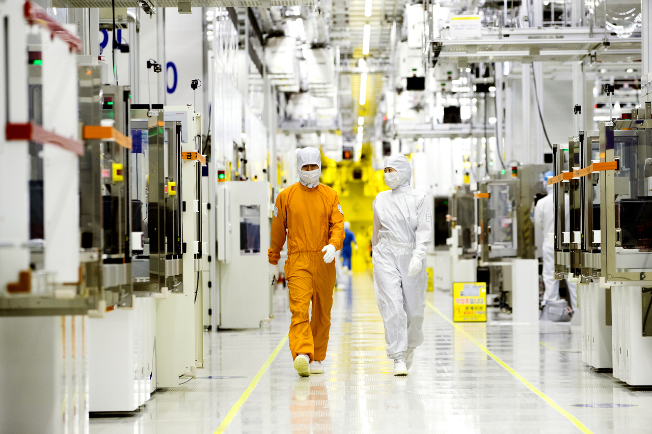
Samsung Electronics said it would invest a record 110 trillion won ($73.5 billion) in facilities and research this year as it moves to secure multiyear supply deals with major AI chip customers, according to a corporate value-up plan disclosed Thursday.
The figure represents a 21.7 percent increase from 2025 and the first time Samsung's annual spending has exceeded 100 trillion won. It is also the largest single-year allocation within the company's previously announced 450 trillion-won, five-year investment roadmap.
Most of the spending will flow to the Device Solutions division, which houses Samsung's semiconductor operations.

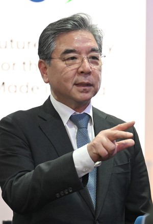
At the company's annual general meeting on Wednesday, Vice Chairman Jun Young-hyun said Samsung is shifting its memory business toward supply contracts of three to five years, replacing the quarterly and annual arrangements standard in the industry.
"If we transition to multiyear contracts, both our customers and Samsung will gain predictable business stability and visibility," Jun told shareholders, adding that such agreements would allow the company to anticipate demand shifts and adjust investment levels more flexibly.
Backing those commitments requires production capacity to match, which is where the record spending comes in.
Building the capacity to back the contracts
Samsung is accelerating construction at its Pyeongtaek campus in Gyeonggi Province, where it is compressing timelines at the P4 fab and installing core equipment for P5. A new plant is also under construction at the Yongin cluster.
In Taylor, Texas, a foundry fab targeting 2-nanometer processes is aiming for commercial production by year-end, after delays that pushed the original 2024 target back by two years. Tesla's next-generation AI chips, under a deal Reuters has reported at $16.5 billion, are reportedly slated for manufacturing at the Taylor facility starting in 2027.
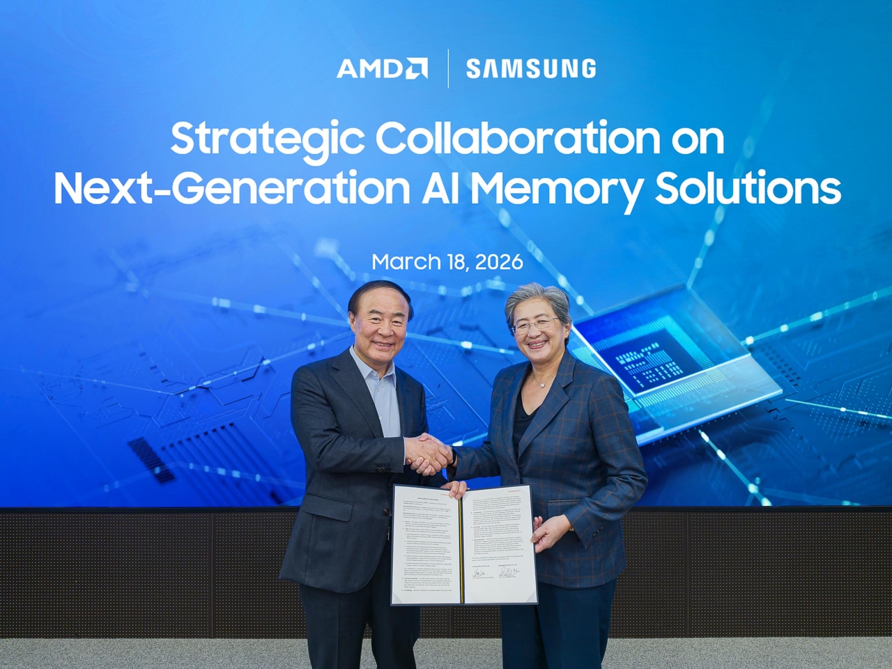
On the memory side, Samsung began mass-producing its sixth-generation high-bandwidth memory, HBM4, in February, becoming the first chipmaker to ship the product. Samsung has since joined Nvidia's HBM4 supply chain and signed an agreement on Wednesday with AMD designating Samsung as a preferred HBM4 supplier for AMD's next-generation data center GPU.
At Nvidia's GTC 2026 conference, Samsung also unveiled its seventh-generation HBM4E, with sample shipments targeted for the second half of this year.
Foundry momentum, with caveats
The foundry business has gained momentum from a run of high-profile customer wins, but it is starting from a diminished base. Samsung's share of the pure-play foundry market fell from 10 percent in the second quarter of 2024 to 7 percent in the fourth quarter of 2025, according to Counterpoint Research.
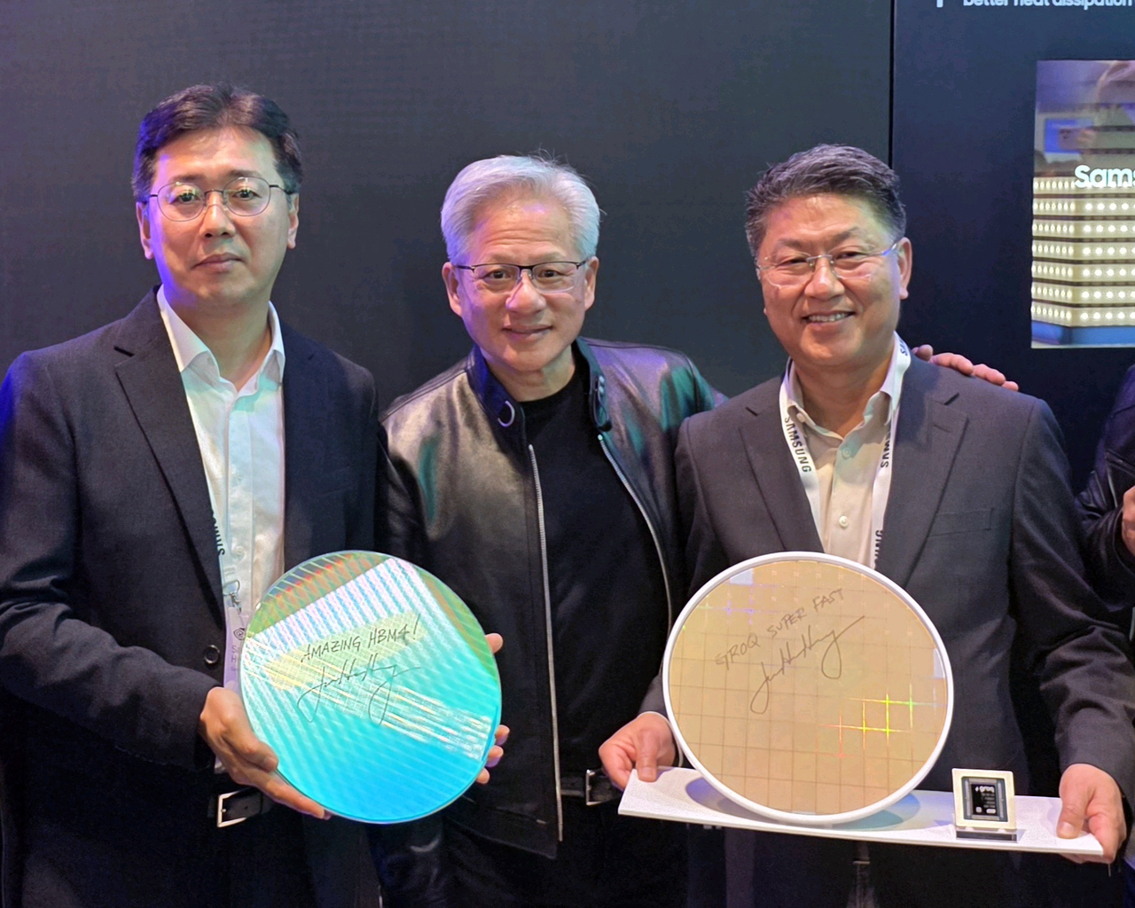
Recent developments suggest a possible inflection. Nvidia CEO Jensen Huang confirmed at GTC on Monday that Samsung is producing the Groq 3 language processing unit on its 4-nanometer process for Nvidia's next-generation AI platform. "We're ramping production as fast as possible. Thank you, Samsung," Huang said.
Han Jin-man, head of Samsung's foundry unit, called the company's Tesla chip contract "a strategic and future-oriented partnership" and told shareholders that Samsung's 2nm process would anchor the Taylor fab's output. He acknowledged, however, that tangible profitability gains for the division are still one to two years away.
Beyond semiconductors, Samsung said it plans to pursue acquisitions in advanced robotics, medtech, automotive electronics and HVAC systems. The company added that any remaining funds from 50 percent of its 2024-2026 free cash flow, after prior payouts and this year's 9.8 trillion-won regular dividend, would be returned to shareholders.
mjh@heraldcorp.com