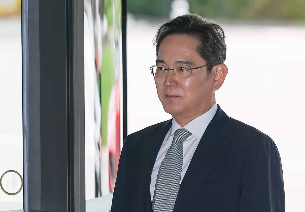
Samsung Electronics Chairman Lee Jae-yong reportedly met with five top executives in Tokyo this week, fueling speculation over the company's semiconductor strategy in Japan and broader business priorities.
According to industry sources Thursday, the executives traveled to Tokyo on Tuesday to meet Lee, who was already in Japan.
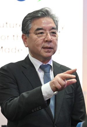
The group included Vice Chairman Chung Hyun-ho, a longtime confidant of Lee; Park Hark-kyu, head of Samsung's business support office; Jun Young-hyun, head of the Device Solutions division overseeing semiconductors; Roh Tae-moon, head of the Device eXperience division overseeing smartphones, home appliances and televisions; and Kim Yong-kwan, president of the DS division.
The rare gathering of Samsung's two major business division chiefs and senior corporate advisers overseas has raised questions about the meeting's agenda, with industry observers suggesting discussions may have extended beyond Japanese operations to companywide priorities.
The meeting follows Samsung's Sept. 8 opening of its Advanced Package Lab in Yokohama, a research facility aimed at strengthening cooperation with Japanese semiconductor materials and equipment suppliers.
Samsung plans to invest 40 billion yen ($253 million) in the facility over five years through 2028. The lab will collaborate with Japanese companies and research institutions on advanced packaging materials and processes for high-bandwidth memory and other next-generation chips.
Jun attended the opening alongside representatives of Japanese partners, including Tokyo Electron and Ibiden. The project has also received support from Japan's Ministry of Economy, Trade and Industry.
Industry observers believe the Tokyo meeting may have included discussions on the lab's operations and further cooperation with Japanese suppliers, which play a critical role in the global semiconductor supply chain. The agenda, however, has not been confirmed.
Samsung is also expanding its research presence in Japan. Its think tank, Samsung Global Research, plans to open a Tokyo office by year-end to monitor economic and industrial trends, government policies and consumer markets. It would be the institute's second overseas office after Beijing.
Lee, who earned a master's degree from Keio University, has long-standing ties with Japanese business leaders. Last month, he hosted visiting Japanese upper-house lawmakers in Seoul for discussions reportedly covering cooperation in AI and semiconductors.
A Samsung official said the company could not confirm details of the executives' trip.
yeeun@heraldcorp.com