Four new southwest memory fabs, HBM packaging hubs aim to double Korea's DRAM capacity, cement AI-era leadership
South Korea is betting nearly 900 trillion won ($583 billion) that the artificial intelligence boom will create enough demand for memory chips to justify building an entirely new semiconductor production belt outside the Seoul metropolitan area.
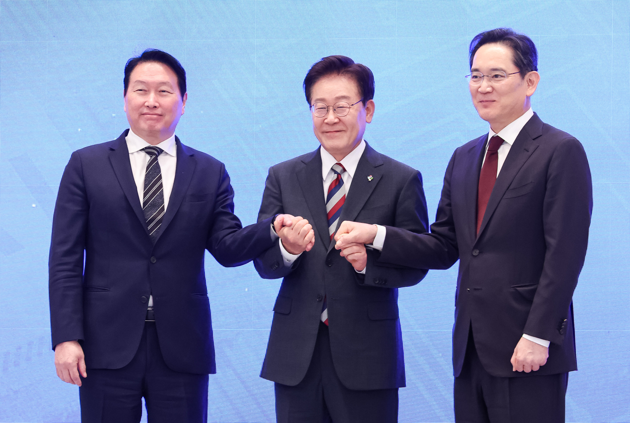
At Monday's presidential public briefing on the government's three megaprojects, Samsung Electronics Chairman Lee Jae-yong and SK Group Chairman Chey Tae-won unveiled investment plans totaling 881 trillion won, including four memory fabs in the southwest and advanced packaging facilities in North and South Chungcheong provinces.
"Companies pursue profit, but they have also shown they can act for the future of the nation," President Lee Jae Myung said, bowing deeply to the two business leaders. "I would like to call these two men national heroes."
The semiconductor initiative aims to double Korea's DRAM production capacity within five years while linking the country's AI-era industrial strategy with Lee's regional development agenda.
To execute the plan, the government unveiled a "3S+1F" strategy centered on speed, stronghold and spearhead, backed by a full-support system involving central and local governments, chipmakers, suppliers and universities.
"Korea can no longer rely on a single capital-region chip belt," Industry Minister Kim Jung-kwan said, calling semiconductors the backbone of the AI era and Korea's "last chance" to escape low growth.
"While projects in Yongin and Pyeongtaek will be accelerated, new growth bases are needed as semiconductor sites face mounting constraints in power, water and land."
Lee also pledged fast-track approvals and one-stop infrastructure support for regional investments, saying he would establish a dedicated presidential team to oversee the projects.
Under the speed pillar, Seoul will fast-track infrastructure and permits for existing projects in the capital region. The government aims to bring forward completion of SK hynix's Yongin general industrial complex by 12 years and Samsung Electronics' Yongin national industrial complex by seven years.
SK hynix's Yongin cluster is targeted for completion by 2033, while Samsung's Yongin project is expected to be completed around 2040.
Under the stronghold pillar, Samsung and SK hynix will each build two memory fabs in Gwangju and the southwest region, with combined investment reaching 800 trillion won. The companies will also invest 81 trillion won in a high-bandwidth memory packaging hub centered on Cheonan and Onyang in South Chungcheong Province.
"Samsung will work to help the Korean semiconductor industry maintain its technological edge," Lee Jae-yong said.
Including previously announced investments in Pyeongtaek and Yongin, Samsung said it plans to invest 2,655 trillion won domestically, including 625 trillion won for new projects in AI chips, robotics, batteries, IT components and materials across Honam, Chungcheong and Yeongnam.
Chey noted that SK hynix's Yongin cluster took nine years to prepare, underscoring the importance of infrastructure and regulatory support for new fabs.
"Demand visible today remains strong. Even with continued investment, it will be difficult to fully resolve supply shortages," Chey said.
He added that SK plans about 1,100 trillion won in semiconductor expansion projects, including existing projects in Yongin and an additional 400 trillion won commitment in the southwest, while pacing spending according to market demand.
The government's bet rests on expectations of explosive AI-driven memory demand. Market tracker Omdia projects the global memory market will quadruple to $800 billion by 2030 from $200 billion in 2025, driven by demand for high-bandwidth memory, AI servers and data-intensive computing systems.
The new southwest fabs, together with the Yongin cluster under construction, are intended to significantly expand Korea's output as rivals race to add capacity. Micron Technology is seeking additional production through its planned acquisition of Taiwan's PSMC and a new fab in Idaho, while China's CXMT is preparing another memory fab in Shanghai.
"For Korea, the memory race is no longer just a contest between chipmakers, but a national competition over infrastructure, supply chains and speed," the Industry Ministry said.
The government also said the Daegu-North Gyeongsang region would be developed into a materials, parts and equipment innovation hub, including for power semiconductors and next-generation chip technologies.
In addition, Seoul plans to invest more than 30 trillion won over the next 15 years to support the entire semiconductor cycle, from research and design to demonstration and manufacturing, for next-generation memory, on-device AI, on-sensor AI and defense semiconductors.
The other two megaprojects announced Monday — physical AI and AI data centers — are intended to prepare Korea for the next phase of AI infrastructure.
Under the physical AI initiative, Seoul plans to build an ecosystem for robots and autonomous systems spanning manufacturing, logistics, defense and healthcare. The government aims to transform Korea from one of the world's largest robot users into a leading robot producer, with humanoid robots deployed across 10 industries by 2028.
The AI data center initiative focuses on large-scale computing infrastructure, including SK Group's 1-gigawatt project in Ulsan, GS Group's 2.4-gigawatt project in Donghae and Naver's expansion in Sejong. The first phase targets 8.4 gigawatts of capacity.
SK also reiterated plans to build 15 gigawatts of AI data center capacity nationwide, led by SK Telecom, starting with 5 gigawatts in areas with available power and land and expanding to 15 gigawatts by 2035 if demand supports further investment.
Experts say the semiconductor ambition will have to be matched by execution.
SK hynix's Yongin cluster broke ground six years after it was announced because of delays involving water supply and land compensation. In semiconductors, even a one- or two-year delay can significantly erode returns if process technologies have already moved on.
Water and talent may prove the biggest hurdles for the southwest expansion. Semiconductor fabs require enormous quantities of water for wafer cleaning and ultrapure water production, while attracting engineers outside the capital region remains a major challenge.
herim@heraldcorp.com