Prototype progress contrasts with steep barriers to mass production
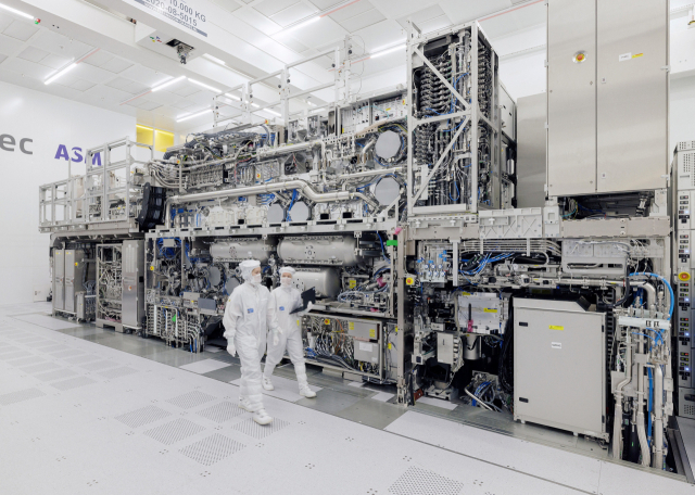
US-led export controls are pushing China to accelerate efforts to develop its own extreme ultraviolet lithography tools, but experts say turning early prototypes into mass-production systems within this decade remains highly unlikely.
China is reported to have built a prototype EUV machine by reverse-engineering older equipment from Dutch supplier ASML, with ambitions to begin mass production by 2028. While a lab-level demonstration is plausible, industry observers say bridging the gap to commercial-scale manufacturing is far more complex.
“For China, a one-off demonstration of a homegrown EUV system is possible,” said Ahn Jin-ho, a materials science professor at Hanyang University. “But developing a system capable of high-volume manufacturing within the next decade is unlikely.”
EUV still out of reach
Without access to cutting-edge EUV lithography — which uses extreme ultraviolet light to etch circuits thousands of times thinner than a human hair — China has relied on deep ultraviolet tools, repeating patterning steps to achieve similar results at higher cost and lower efficiency.
But DUV can only take China so far. As Samsung and TSMC push toward 2-nanometer chips, Beijing has launched a state-backed EUV effort, reportedly recruiting former ASML engineers and ramping up investment.
“Below 7-nanometer nodes, EUV lithography is effectively indispensable,” said Ahn Ki-hyun, executive director of the Korea Semiconductor Industry Association. “If China succeeds in localizing EUV, it could reshape the chip landscape. But it won’t happen overnight.”
Ahn Jin-ho, an EUV expert at Hanyang University who recently received an award from the National Academy of Engineering of Korea, is highly skeptical that China can deliver a mass-production EUV system by its 2028 target.
“Industry heavyweights like Nikon and Canon, which long dominated lithography, never cracked EUV. This is not a technology you can brute-force your way into,” Ahn said.
Even for ASML, the sole supplier of EUV systems, development took decades and relied on a tightly coordinated ecosystem, including precision optics from Carl Zeiss and specialized light-source technologies, he added.
The optics system remains one of the biggest hurdles, requiring extraordinary precision in both design and manufacturing. Equally critical is the integration of the broader ecosystem — including masks, pellicles and photoresists — all of which must function seamlessly with the tool.
“Achieving that level of optimization — from particle control to managing hydrogen environments inside EUV systems — takes decades of accumulated know-how,” Ahn said.
China has advanced chipmaking using older lithography tools and ArF immersion, repeating patterning steps to reach what it claims are near 3-nanometer capabilities, though most production at cutting-edge nodes remains around the 7-nanometer level.
But that workaround comes at a cost. Companies such as ChangXin Memory Technologies, Yangtze Memory Technologies and Semiconductor Manufacturing International Corporation face mounting financial pressure as multiple patterning drives up production expenses.
“In manufacturing, it is all about cost and profit. If you need multiple exposures just to match what EUV can do in one, the economics simply don’t work,” an industry official said.
Samsung, SK widen EUV lead
EUV systems — comprising more than 100,000 components — typically cost around $200 million to $300 million per unit. ASML produces only about 70 units annually.
Samsung recently ordered roughly 20 of the scarce EUV machines from ASML as part of a broader 70-unit lithography purchase for its P5 fab in Pyeongtaek, Gyeonggi Province, with the EUV portion alone estimated at more than 10 trillion won ($7.3 billion).
SK hynix has also committed about 11.9 trillion won to EUV tools to be installed at its Cheongju M15X fab and upcoming Yongin fabs, with deliveries through end-2026.
The companies are expected to use the EUV systems to support their AI memory production, including next-generation high-bandwidth memory.
Scale alone does not guarantee an edge. EUV tools are typically used only for the most critical layers, and their impact depends heavily on how effectively they are integrated into the manufacturing process.
"Even with the same tools, outcomes can vary. Component differences, tool condition and operator experience all affect yield and quality," Ahn of Hanyang University said.
"Chipmakers rely on a mix of EUV, ArF and KrF, and decisions on where to deploy each technology also shape both performance and cost competitiveness," he added.
herim@heraldcorp.com