President Lee says four-month push by government, industry is turning ambitious investment pledges into reality
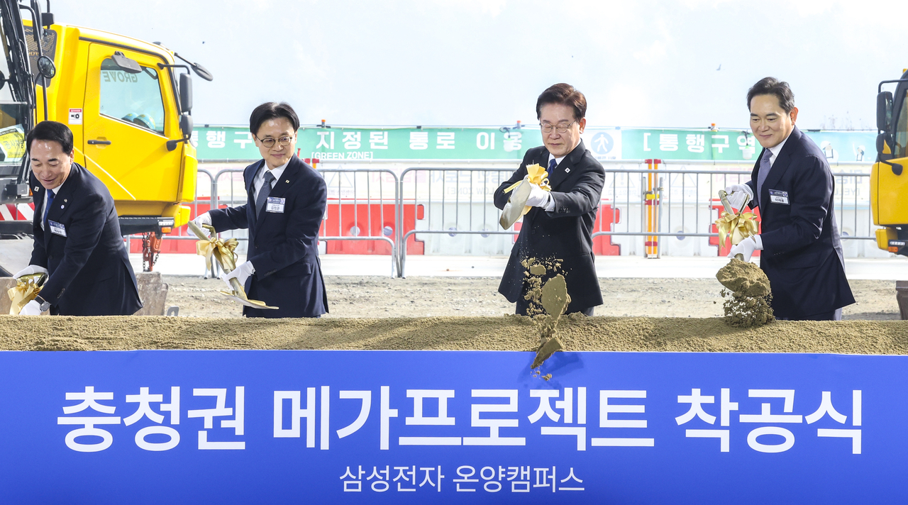
South Korea broke ground Thursday on the first project under its flagship industrial megaproject initiative at Samsung Electronics’ advanced chip packaging facility, just four months after the government unveiled the plan.
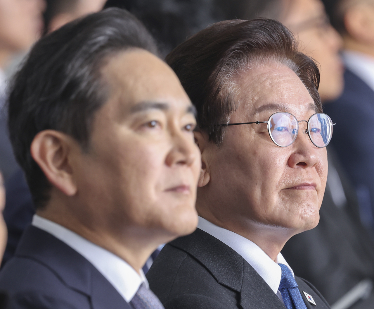
President Lee Jae Myung joined Samsung Electronics Chairman Lee Jae-yong at the company's Onyang campus in Asan, South Chungcheong Province, where a decades-old semiconductor assembly and testing operation is being transformed into a hub for advanced high-bandwidth memory packaging.
“Just four months later, we are standing at the site where that promise is becoming reality,” President Lee said.
The groundbreaking marks a milestone for the government's three megaprojects unveiled in late June that seek to cultivate new growth engines in semiconductors, AI data centers and physical AI while steering investment beyond the Seoul Metropolitan Area.
In July, Samsung Electronics, SK Hynix and other major companies unveiled plans to invest roughly 392 trillion won ($295 billion) in the central Chungcheong region as part of a series of regional investment announcements held across the country.
Speaking at the ceremony, President Lee highlighted Samsung’s plans to build a 6 trillion won advanced semiconductor packaging fab at Onyang, followed by 40 trillion won in phased investments in advanced equipment.
“The Onyang campus here in Asan will become a key hub for advanced HBM packaging,” he added
Samsung Chairman Lee traced the site's evolution from barren hills and unpaved roads four decades ago to a major semiconductor assembly and testing center.
"With today's groundbreaking, we pledge to take another leap forward," he said. "This site, once primarily focused on assembling and testing conventional semiconductors, will be transformed into a cutting-edge HBM hub at the heart of AI semiconductors."
Samsung Electronics Vice Chairman Jun Young-hyun outlined progress on the group's regional investments.
Samsung has moved up construction of Onyang Line 5 by about a year, targeting operations in June 2028. The three-story plant will house about 31,000 square meters of cleanroom space and produce next-generation HBM4E chips, as surging demand for AI memory strains global supplies.
The investment represents a significant shift for Onyang, traditionally a center for semiconductor assembly and testing, toward advanced packaging technology that has become increasingly critical to artificial intelligence computing.
Lee thanks Samsung, local govts
In his speech, President Lee thanked Chairman Lee, who sat beside him during the ceremony, and Samsung executives for their “bold investment decisions and swift execution.”
Lee further underlined that the South Chungcheong Provincial government and the city of Asan had shortened permitting times to roughly one-third of their usual duration, allowing construction to move ahead swiftly.
“This is a model example that clearly demonstrates how quickly things can change on the ground when local governments take an active role,” Lee said.
The president pledged that central and local governments would work together to secure necessary permits and develop essential infrastructure, including electricity and water supplies, to ensure that all planned investments across the country proceed without disruption.
President Lee further emphasized that the investments should do more than expand corporate manufacturing facilities outside the Seoul metropolitan area.
"Above all, what matters is that those living here should also share in the benefits of these massive investments," he said.
The president pledged to mobilize the government's policy resources to ensure that the projects create opportunities for smaller businesses and allow young people to build careers in their home regions.
At the event, Kim Young-jae, chairman of Samsung supplier Daeduck Electronics, said 194 South Korean companies specializing in semiconductor materials, parts and equipment, including Daeduck, plan to invest a combined 18.1 trillion won by 2030.
Of those, 66 companies in the Chungcheong region are investing or preparing to invest 4.4 trillion won, he said. The investments are expected to create about 23,000 jobs.
Lee pleges support to turn investments into results
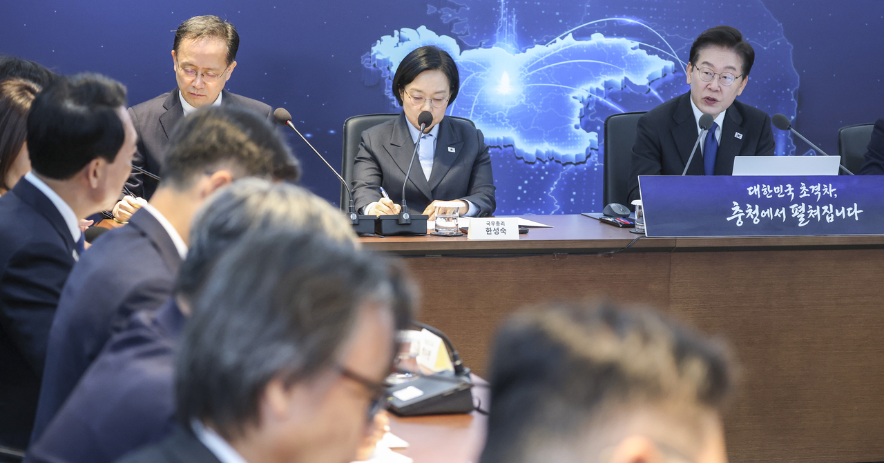
At the fourth public-private review meeting on the megaproject initiative following the ceremony, President Lee emphasized that "the government and businesses have gone beyond moving at full speed to mounting an all-out effort" over the past four months.
"Changes are increasingly becoming visible on the ground," Lee added during the meeting held at Samsung's Onyang campus.
Six of the eight companies participating in the Chungcheong initiative have begun implementing their investment plans, while projects in the Honam and Yeongnam regions are also making progress, Lee said.
"What is even more encouraging is that as the megaproject investments get underway, materials, parts and equipment suppliers linked to major companies are making additional investments," Lee added.
Lee said 112 companies in sectors including semiconductors and biotechnology are expected to invest an additional 23.6 trillion won in the Chungcheong region, on top of the 392 trillion won originally planned.
Lee pledged that "the government will also actively support companies' efforts to ensure they deliver tangible results on the ground."
"What matters now is action, not words. Implementation, not promises," he added.
dagyumji@heraldcorp.com