TSMC’s CoWoS-L is set to dominate through 2028, while Samsung Electro-Mechanics and LG Innotek prepare for alternatives
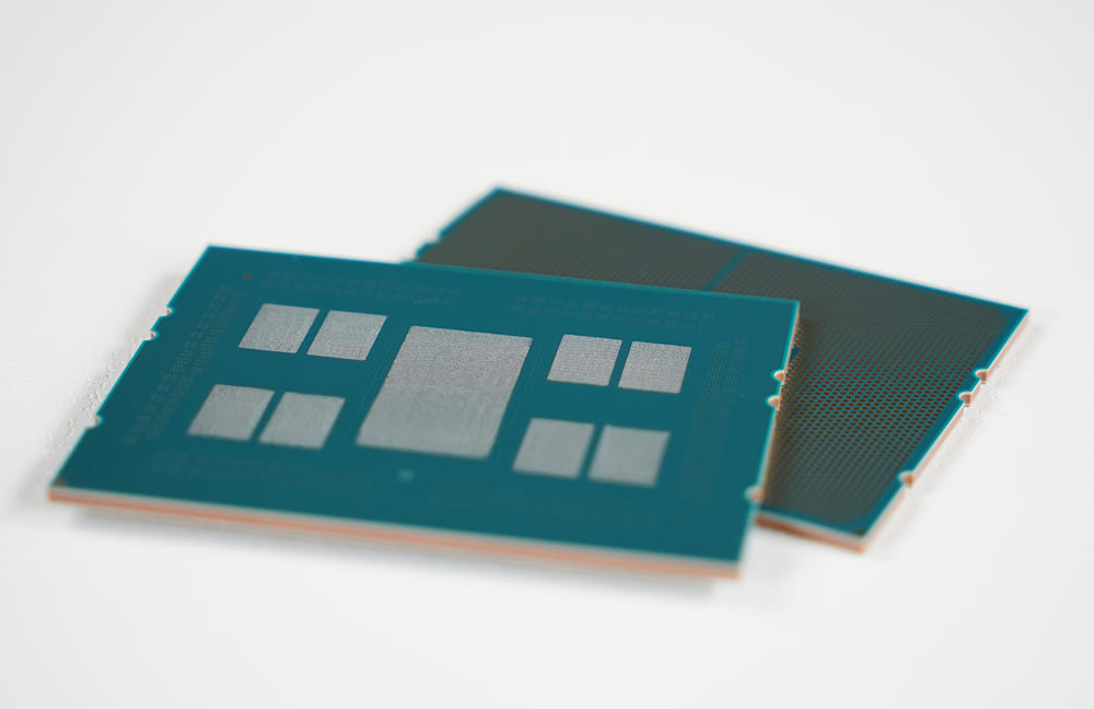
Taiwan Semiconductor Manufacturing Co.'s advanced packaging technology, chip-on-wafer-on-substrate-L, or CoWoS-L, remains the dominant force in AI semiconductor packaging.
But Korean chip substrate makers are already preparing for the next market shift.
Samsung Electro-Mechanics and LG Innotek are strengthening their capabilities in advanced semiconductor substrates, including technologies related to Intel’s embedded multi-die interconnect bridge, or EMIB, an advanced packaging that offers an alternative to TSMC's CoWoS technology.
The move does not indicate that Korean companies expect TSMC’s current advantage to disappear soon. Rather, it reflects a broader industry shift as AI chips become larger, architectures become more complex and customers seek different packaging solutions.
Market research firm TrendForce forecasts that CoWoS-L will remain the mainstream AI packaging technology through at least 2028, supported by TSMC’s manufacturing experience, customer base and expanding production capabilities.
CoWoS-L remains center of AI packaging
The AI semiconductor race is moving beyond chip design and manufacturing processes toward advanced packaging.
High-performance AI accelerators combine graphics processing units, high-bandwidth memory and multiple computing dies in a single package. Efficiently connecting these components has become a key factor in improving performance and power efficiency.
TSMC’s CoWoS technology currently dominates the high-end AI accelerator market. Nvidia and other major AI chip developers rely on TSMC’s advanced packaging capabilities to integrate logic chips with HBM.
The latest CoWoS-L architecture was developed as AI packages grew larger and required greater integration of memory and computing components.
Unlike earlier approaches that relied heavily on large silicon interposers, CoWoS-L uses silicon-based connection structures only where necessary, allowing larger package designs while addressing some cost and scalability challenges.
With a mature ecosystem and extensive manufacturing experience, TSMC is expected to maintain its strong position in AI packaging for the foreseeable future.
However, the rapid expansion of AI infrastructure is also creating new challenges. Larger packages, higher power consumption and increasing chip complexity are pushing the industry to explore additional approaches.
EMIB emerges as future packaging option
Intel’s EMIB has emerged as one technology being watched by semiconductor substrate makers.
Unlike conventional approaches that use large silicon interposers, EMIB connects chips through small silicon bridges embedded inside the substrate. The structure can reduce dependence on large silicon components and provide greater flexibility for complex package designs.
Intel has also developed EMIB-T, an enhanced version designed to improve power delivery performance for high-performance applications such as AI semiconductors.
Industry observers do not expect EMIB-T to replace CoWoS-L in the near term. TSMC still holds a significant advantage in commercial adoption, manufacturing scale and customer ecosystem.
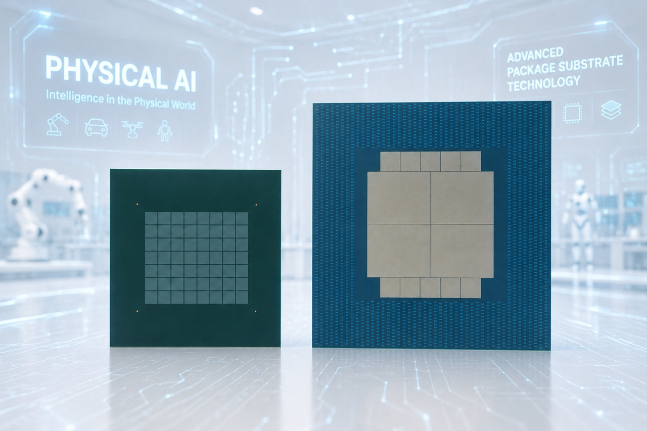
For Korean substrate makers, however, EMIB represents preparation for a market where multiple packaging architectures could coexist depending on performance requirements, cost considerations and supply-chain strategies.
Korean firms keep multiple technology paths open
Samsung Electro-Mechanics’ development of 2.1D and 2.5D packaging substrate technologies reflects this changing market environment.
“Unlike standardized products, semiconductor substrates are developed according to customer requirements,” an industry source familiar with Samsung Electro-Mechanics said.
“That means companies cannot focus on only one technology. They need to keep multiple options open because it remains uncertain which packaging approach will gain wider adoption,” the source added.
The source added that Samsung Electro-Mechanics is preparing next-generation substrate technologies beyond current FC-BGA solutions, including advanced packaging substrates and glass substrates.
“Substrate makers need to strengthen existing businesses while preparing technologies for the next generation of packaging,” the source said.
LG Innotek is also expanding its capabilities in high-end FC-BGA substrates targeting AI servers and data centers.
As AI accelerators become larger, package substrates must support larger areas, higher layer counts and increasingly complex circuit designs. Improving fine circuit formation, layer accuracy and warpage control has become a critical challenge.
“AI packaging is unlikely to develop around a single technology,” an industry source said.
“Different solutions could coexist depending on customer requirements and chip architectures,” the source added.
For Samsung Electro-Mechanics and LG Innotek, preparing for EMIB-related technologies is less about challenging TSMC’s current leadership and more about keeping pace with a rapidly changing AI packaging market.
yeeun@heraldcorp.com