To address the challenges to meet the pressing requirements of next-generation data processing and storage systems, Samsung has introduced new Vertical-NAND memory solutions and technology to its global customers.
At this year’s Flash Memory Summit held in Santa Clara, California, in August, Samsung showcased solutions to address next-generation data processing challenges centered around the company’s latest V-NAND technology and an array of solid state drives. The company hopes SSDs will be at the forefront of enabling today’s most data-intensive tasks such as high-performance computing, machine learning, real-time analytics and parallel computing.
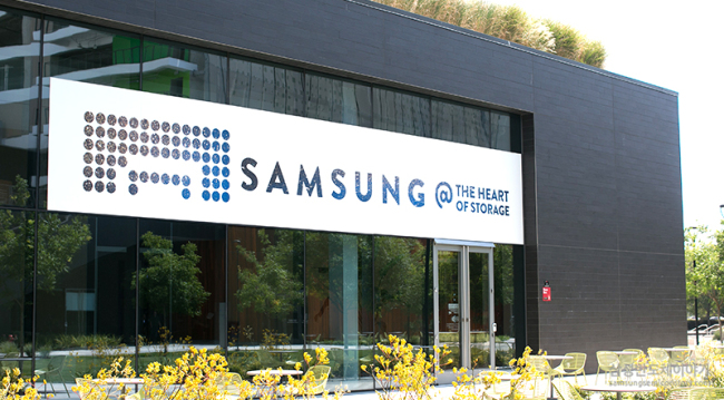
A banner presents the main theme of the 2017 Flash Memory Summit, “Samsung @ The Heart of Storage,” at the building of Samsung Semiconductor Inc. in Silicon Valley in August. (Samsung Electronics)
Jeong Jae-heon, executive vice president of Samsung’s solution development, introduced the company’s new V-NAND chip fabrication line in Pyeongtaek, Gyeonggi Province, to around 1,000 industry officials in the US, in his keynote speech at the summit.
With the rapidly increasing data-intensive applications across industries using artificial intelligence and Internet of Things technologies, the role of flash memory has become critical in accelerating the speed at which information can be extracted for real-time analysis.
Samsung’s device solutions business, focused on memory chip production is the largest division of the South Korean tech giant, which accounted for more than 70 percent of the company’s entire operating profits for the first half of this year.
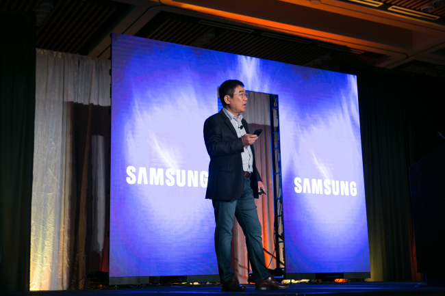
Jeong Jae-heon, executive vice president of solution development at Samsung Electronics, delivers a keynote speech at the 2017 Flash Memory Summit in Santa Clara on Aug. 8. (Samsung Electronics)
Samsung announced it will launch a 1-terabit (Tb) V-NAND chip next year, which will mark the industry’s first single NAND chip using a three-dimensional structure.
The arrival of a 1Tb V-NAND chip next year will enable 2-terabytes (TB) of memory to be put in a single V-NAND package by stacking 16 1Tb dies and will represent one of the most important memory advances of the past 10 years, the company said.
“Our new, highly advanced V-NAND technologies will offer smarter solutions for greater value by providing high data processing speeds, increased system scalability and ultra-low latency for today’s most demanding cloud-based applications,” said Jin Gyo-young, executive vice president and head of memory business at Samsung Electronics. “We will continue to pioneer flash innovation by leveraging our expertise in advanced 3D-NAND memory technology to significantly enhance the way in which information-rich data is processed.”
Samsung also said it is sampling the industry’s first 16-TB next generation small form factor (NGSFF) solid state drive, which will improve the memory storage capacity and input/output operations per second (IOPS) of today’s rack servers. The Samsung NGSFF SSD provides large data center servers with substantially improved space utilization and scaling options.
Utilizing the new NGSFF drive instead of M.2 drives can increase the storage capacity of a server of the same size.
To highlight the advantages, Samsung demonstrated a reference server system that delivers a total of 576 terabytes in a 1U rack unit, the smallest standard unit for a server rack, using 36 16TB NGSFF SSDs. The 1U system can process about 10 million random read IOPS, Three times more than a 1U server equipped with 2.5-inch SSDs. A petabyte capacity can be achieved using only two of the 576TB systems.
Samsung plans to begin mass producing its first NGSFF SSDs in the fourth quarter of this year, while working to standardize the form factor with industry partners.
By Song Su-hyun (song@heraldcorp.com)


![[Exclusive] Korean military set to ban iPhones over 'security' concerns](http://res.heraldm.com/phpwas/restmb_idxmake.php?idx=645&simg=/content/image/2024/04/23/20240423050599_0.jpg&u=20240423183955)


![[Herald Interview] 'Amid aging population, Korea to invite more young professionals from overseas'](http://res.heraldm.com/phpwas/restmb_idxmake.php?idx=645&simg=/content/image/2024/04/24/20240424050844_0.jpg&u=20240424200058)