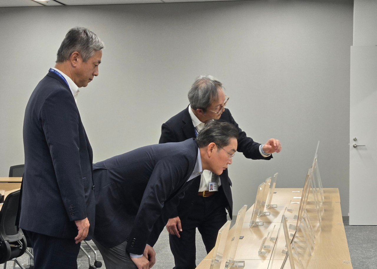
Samsung Electronics Executive Chair Lee Jae-yong visited the company's advanced semiconductor packaging research facility in Japan on Sunday, emphasizing the need to secure cutting-edge packaging technologies to sharpen its competitive edge in AI chips.
Lee inspected the Advanced Package Lab in Yokohama, where he reviewed progress in developing next-generation packaging materials and manufacturing processes with local researchers. He also discussed ways to strengthen cooperation with Japan’s semiconductor materials, components and equipment suppliers, the company said Sunday.
The visit coincided with the 57th anniversary of Samsung Electronics’ founding, highlighting Lee’s focus on technological development rather than holding a separate anniversary event.
It also marked his first visit to the facility since its official opening on Sept. 8, stressing the growing strategic importance of advanced packaging in the global AI semiconductor race.
Established in 2023, APL officially opened in September as Samsung's research hub for developing and validating core materials and manufacturing processes used in advanced semiconductor packaging. The company plans to invest 350 billion won ($262 million) in the research and development facility over five years through 2028.
Samsung aims to develop the facility into a global R&D hub for next-generation packaging technologies, including advanced bonding processes and glass substrates.
The lab is also expected to work closely with Samsung's semiconductor research operations in South Korea, combining the company's chip design and manufacturing expertise with Japan's strengths in semiconductor materials, components and equipment.
The company also aims to develop APL into a research collaboration hub linking Samsung's semiconductor expertise with Japanese materials and equipment suppliers, leveraging Yokohama's skilled workforce and extensive network of universities, research institutions and industry partners.
sahn@heraldcorp.com