Samsung, SK, Micron race to meet tighter technical demands as Nvidia accelerates AI road map
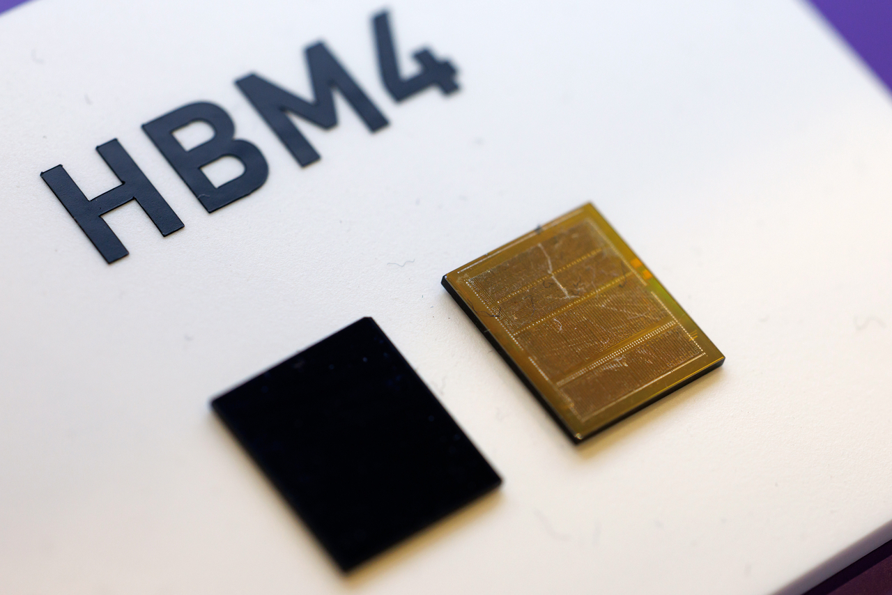
Nvidia has reportedly begun testing the limits of the global AI memory supply chain by signaling interest in 16-layer high-bandwidth memory for delivery as early as late 2026, forcing Samsung Electronics, SK hynix and Micron Technology into a race to meet the requirements of next-generation AI accelerators.
According to industry sources, Nvidia has recently asked major memory suppliers whether they could deliver 16-layer HBM in the fourth quarter of 2026. The discussions remain exploratory, with no contracts signed, but they have triggered internal planning around development schedules, yield targets and initial production volumes.
Some suppliers expect performance evaluation to begin before the third quarter of 2026.
The inquiry comes as Nvidia prepares to scale production of 12-layer HBM4, the current focus of supplier qualification. Sources said the move toward 16 layers is pulling forward the generational transition, even before 12-layer HBM4 reaches full commercial rollout, which is still expected in early 2026. The 16-layer product is still expected to be classified as HBM4, although the naming could shift to HBM4E depending on final specifications and timing.
“Nvidia upgrades its GPUs very aggressively, and HBM has to advance at the same pace,” said Ahn Ki-hyun, executive vice president of the Korea Semiconductor Industry Association and a former employee from SK hynix. “If memory performance can't keep up, even a higher-performance GPU loses its meaning.”
“The transition from 12 to 16 layers is technically much harder than from 8 to 12,” Ahn said. “At that point, it is not just adding layers. In many cases, the manufacturing process itself has to change.”
Industry estimates show that implementing 16-layer HBM requires wafer thickness to be reduced to around 30 micrometers, compared with about 50 micrometers for current 12-layer designs. JEDEC, the global semiconductor standards body, caps HBM4 package thickness at 775 micrometers, leaving limited room for further scaling through conventional approaches.
Those constraints place bonding technology at the center of the transition. Samsung Electronics and Micron currently rely on thermal compression bonding, while SK hynix uses its mass reflow molded underfill process.
Samsung has indicated it is considering the introduction of hybrid bonding starting with its seventh-generation 16-layer HBM4E.
“Samsung is focusing on hybrid bonding early because it struggled to match rivals in current adhesive-based technologies,” Ahn said. “SK hynix is managing its pace. It is developing hybrid bonding as a backup, while aiming to maximize its industry-leading MR-MUF technology for as long as possible.”
Despite the forward-looking focus, the near-term market remains anchored in HBM3E. Analysts at LS Securities estimate HBM3E will account for 66 percent of total HBM output in 2026, down from 87 percent this year but still the clear majority.
The competitive inflection point is expected with the launch of Rubin, Nvidia’s next-generation AI accelerator scheduled for release in the second half of 2026. Each Rubin processor is expected to use eight HBM4 stacks.
Samsung has recently received favorable feedback in Nvidia’s HBM4 system-in-package tests. SK hynix, meanwhile, has already established an HBM4 mass production framework and has been supplying paid samples to Nvidia.
mjh@heraldcorp.com

![[Graphic News] S. Korea ranks 9th in noodle consumption](https://wimg.heraldcorp.com/news/cms/2026/09/29/news-p.v1.20260929.e3945338add94d57ab3f00f8e6781416_T1.gif?type=h&h=800)