South Korea on Wednesday unveiled a semiconductor investment blueprint worth almost half a trillion dollars, with a shift toward artificial intelligence processors and a new industrial corridor in the south of the country.
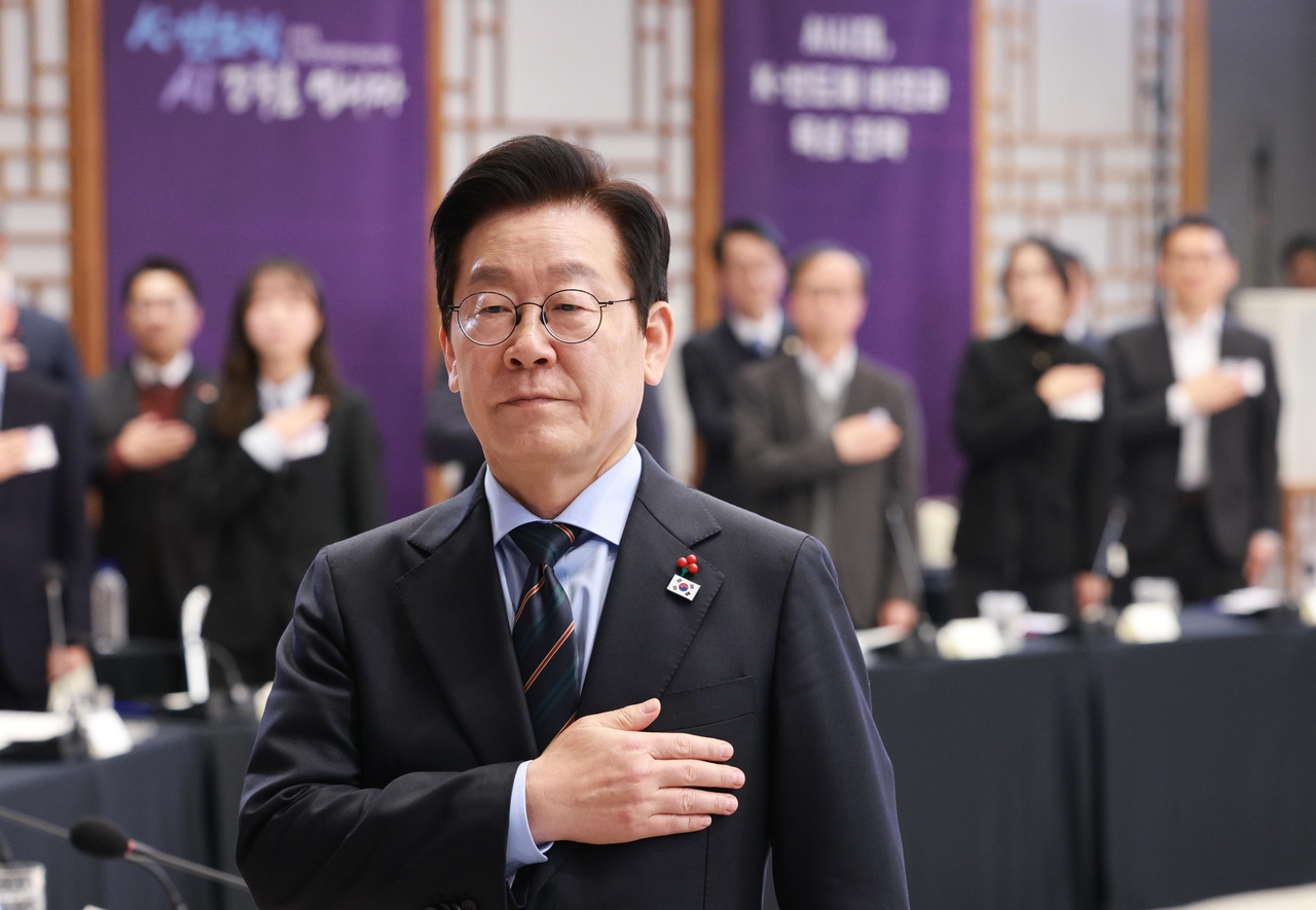
At a meeting in the presidential office Wednesday, Industry Minister Kim Jung-kwan briefed President Lee Jae Myung on a broad government strategy to ensure a competitive edge in the AI industry with private sector investment.
The plan included a 700 trillion won ($475.8 billion) package to construct 10 new semiconductor fabs by 2047, bringing production capacity to 7.9 million 200-millimeter wafers per month.
“As we envision a new leap forward, I believe industrial economic development is key to achieving this. Semiconductors, in particular, are a promising area where we have a strong competitive edge,” Lee said at the meeting, which brought together about 40 semiconductor industry representatives, experts and government officials.
Kim said the plan, comprising investment pledges from the private sector, will be supported by the government's fast-track deregulation and guarantees of a stable water supply through the introduction of a special law that is in the process of being legislated.
The government also outlined new research and development investments in the semiconductor sector, with most going toward AI processing chips, a largely undeveloped field in a country that has so far specialized in the memory sector. By R&D area, 1.27 trillion won in funding will go toward AI chips, 215.9 billion won to developing next-generation memory chips, and a combined 620 billion won toward compound semiconductors and chip packaging.
Additionally, it is reviewing a 4.5 trillion won investment for a foundry project capable of contract manufacturing using 40-nanometer technology under a public-private partnership, designed to support fabless chip designers.
During the briefing, Lee emphasized the need for the domestic chip industry to reduce its reliance on imports across the supply chain, saying this goal could be achieved through balanced regional growth. This aligns with his administration’s proposal to establish a new semiconductor cluster in the southern part of the country.
Under the plan, a semiconductor packaging cluster will be built in Gwangju. Busan will develop a new hub for power semiconductors, while Gumi, North Gyeongsang Province, will focus on manufacturing chip components. These three cities will be linked to form an industrial belt, according to the government.
This is in addition to a chip cluster currently under construction in Yongin, Gyeonggi Province, and another stretching from Cheonan, South Chungcheong Province, to Pyeongtaek, Gyeonggi Province.
Lee stressed that industry participation — particularly companies setting up operations in the south — was crucial to the initiative’s success.
“I hope you will turn your attention to the southern region, which is rich in renewable energy, and take an interest in building a new industrial ecosystem in that region,” he said.
Lee’s five-year policy blueprint, released in August, projects that chip-related exports will increase by 20 percent from 2024 to 2030, surpassing $170 billion. The plan also aims to foster at least 10 AI chip manufacturing firms by 2030.
The blueprint further identifies the development of world-leading technologies for AI chips and high-bandwidth memory as key priorities, pledging to strengthen R&D efforts in neural processing units and processing-in-memory chips.
consnow@heraldcorp.com