After a joint announcement with the South Korean government to make the country the world’s top semiconductor powerhouse last month, Samsung Electronics is gearing up to globalize its efforts to become the No. 1 chipmaker both in the memory and non-memory markets by 2030.
(Samsung Electronics)
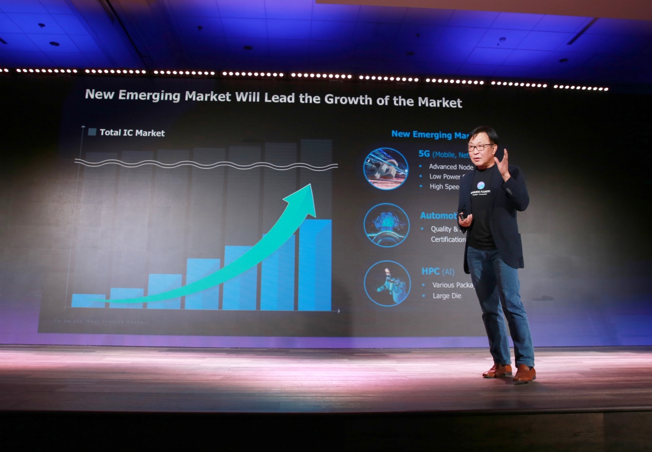
Starting with the annual Samsung Foundry Forum held Tuesday in California’s Silicon Valley, Samsung is planning to proclaim its blueprint to take the lead in the non-memory market in five countries.
The forum takes place in major markets every year for the firm’s fabless customers, but the regular event drew unprecedented attention this year after Samsung’s massive investment plan worth up to 133 trillion won ($111.85 billion) by 2030 was announced.
At the Silicon Valley conference, Samsung not only emphasized its investment plans but also the newest foundry process technologies to attract more global customers.
(Yonhap)
Among them, the architectural successor to the current FinFET, known as get-all-around, or GAA, stole much of the attention.
Samsung is planning to introduce the four-dimensional GAA architecture for the upcoming 4-nanometer process, and below which is an advancement from the current three-dimensional FinFET technology.
The Korean chipmaker has been utilizing the FinFET structure, so its transition to GAA is a major change.
The GAA technology features a gate for transistors on all four sides of the channel to overcome performance limitations and supply voltage of FinFET that features three sides.
Samsung has been developing its proprietary GAA technology, known as multibridge-channel FET since 2002. In comparison with other GAA technologies, Samsung’s is aimed at enhancing gate control and the performance of transistors.
“How perfectly Samsung will come up with the GAA technology would be at the center of the fabless industry’s interest,” said an industry official.
The chipmaker also announced its roadmap for its logic chip and foundry businesses until 2030, including plans to hire 15,000 engineers for research and development and build new cutting-edge foundry facilities by investing around 11 trillion won each year.
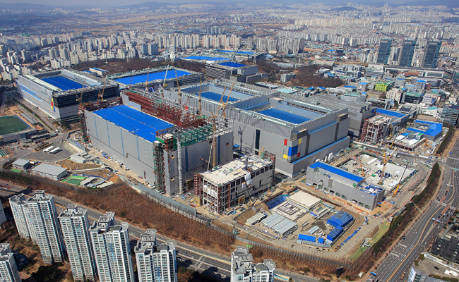
In addition to the extreme ultraviolet lithography equipment line under construction in Hwaseong, Gyeonggi Province, Samsung will build another EUV line at Pyeongtaek in the same province.
Samsung has been manufacturing memory chips at the world’s single largest memory fabrication line at Pyeongtaek since July 2017. For the past 2 1/2 years of a super cycle in the memory market until the fourth quarter last year, Samsung was widely expected to add two to three more memory plants at Pyeongtaek under its 180 trillion won worth investment plan announced in August 2018.
Details of the new Pyeongtaek foundry plant construction are not released yet.
It was instead briefly mentioned by Samsung Vice Chairman Lee Jae-yong during President Moon Jae-in’s tour of Samsung’s EUV line construction site in Hwaseong on April 30.
“While the Hwaseong EUV line is expected to be used for 7 nm, 5 nm and 4 nm processes when it is completed and starts operations next year, the Pyeongtaek foundry line would be spared for next-generation technologies like 3 nm,” said an industry watcher.
Besides the long-term plans, Samsung is reinforcing the current business portfolio of system chips by adding new products to existing lineups.
The company debuted image sensor ISOCELL Bright GW1, featuring the highest resolution of 64 megapixels among mobile image sensors, and GM2, boasting the smallest 48-megapixel sensor in the global market.
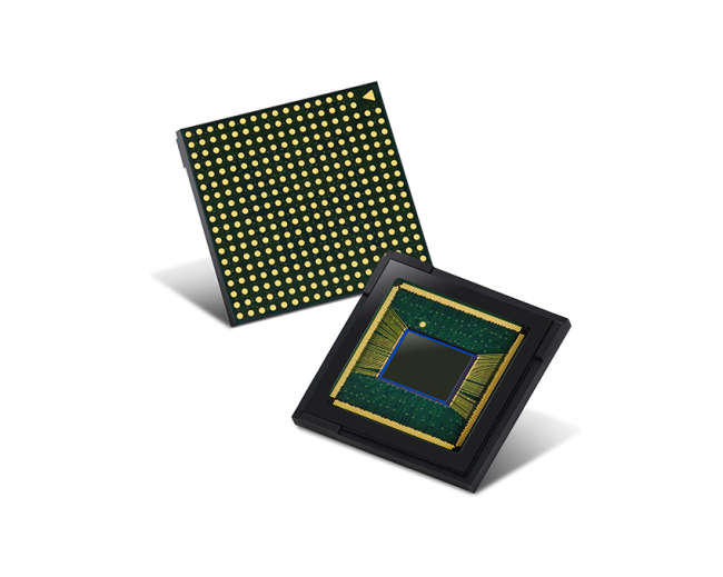
ISOCELL Bright GW1 (Samsung Electronics)
Earlier, Samsung announced the completion of internet of things chips lineup named Exynos i. The tech firm said it will launch IoT processor T100 that is optimized for short distances of within 100 meters, to be used for smart control of appliances and utilities at home.
Samsung’s system chip portfolio also includes the mobile application processor, automotive processor and 5G modem solution.
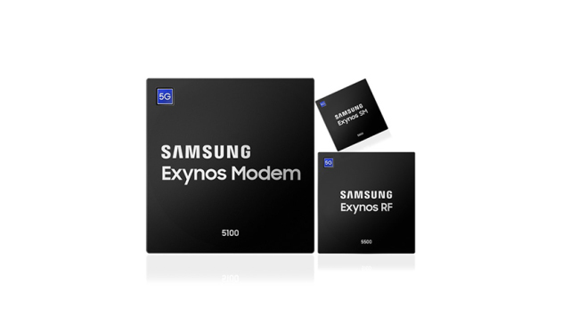
5G modem solution (Samsung Electronics)
By Song Su-hyun (
song@heraldcorp.com)


![[Graphic News] More Koreans say they plan long-distance trips this year](http://res.heraldm.com/phpwas/restmb_idxmake.php?idx=645&simg=/content/image/2024/04/17/20240417050828_0.gif&u=)
